The program division Optical Materials develops novel optical and electro-optical composite materials. These have specific interactions with light as a functionally essential and value-adding function. They are used in bulk materials or as coatings for glass, ceramic, metal, and polymer substrates. The group’s expertise ranges from modeling, the application of wet chemical processes for the synthesis of organic-inorganic matrices to the production of nanoparticles with specific chemical modification and design. The focus is on the development and improvement of application and structuring techniques in industrial and product-related research areas. We cooperate with internal program divisions, the InnovationCenter INM, and the Saarland University. We are contact partners for German and international universities and research institutes as well as for industrial partners from Germany, Europe, and overseas.

Contact
Deputy Head

Secretary

Team Members
Research
Novel Materials for Optical Systems
Carrying out committed basic research on the topic of novel phenomena and effects between materials and electromagnetic radiation and utilizing these results through applications in research and development projects with industrial partners are the complementary goals of the program division.
Innovation from Basic Research
The fundamental research goals of the program division are the validation of photochemical metallization, the development of novel plasmonic structures from silver colloids, electrospinning, integrated optics and biophotonics, and the synthesis of new materials with special refractive indices.
Flexible, transparent conductive layers
Transparent, electrically conductive layers are used as transparent electrodes in many applications, e.g. in displays, touch screens, image screens, and solar cells as transparent electrodes – up to now they have been produced by ITO (indium tin oxide) sputtering as standard. Future flexible displays require flexible electrodes. The Optical Materials program division focuses on the development of flexible, transparent conductive layers through innovative implementation of new technical processes: The photometallization process developed at INM generates silver structures on a photocatalytic base layer, e.g., via mask exposure. The metal structures obtained are very fine, transparent, and electrically conductive. The novel approach of electrospinning produces long, thin polymer fibers with an exceptionally high aspect ratio, which are metalized by an innovative INM process and can be scaled up to the m² range. Wet-chemically produced printed transparent conductive oxide layers (TCO) and structures based on TCO nanoparticles (e.g. ITO), or the use of silver nanowires complete our portfolio. All variants enable the basic use in printed electronics and on flexible substrates.
Photometallization – light-controlled deposition of thin silver layers
Photometallization is a process for the light-controlled deposition of thin silver layers on rigid and flexible substrates. The basis for this is a few nanometers thin, transparent precoating of the substrate with photocatalytically active nanoparticles. When this surface, activated in this way, is brought into contact with a solution of a suitable silver complex and illuminated with ultraviolet light, complex molecules are degraded and the metallic silver released is deposited on the surface. The resulting silver film can reach a thickness of more than 100 nm and a sheet resistance of less than 0.3 Ohm/sq. Exposure is through a mask, but microstructures can also be created by restricting the spread of the silver complex solution or photocatalytic precoating. Based on gratings with mesh sizes of 350-500 µm and line widths of 3-5 µm, functional capacitive multitouch sensors with a net transparency of more than 90 % could be demonstrated on glass and PET substrates. Even after several years of development work, basic principles of layer deposition are still an important topic of ongoing research.
Step 1: A thin transparent layer of a nanoparticulate photocatalyst is applied to a substrate.
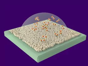
Step 2: The photocatalyst layer is brought into contact with a solution containing a specific silver complex.
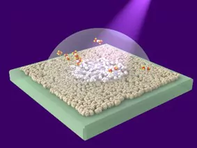
Step 3: Irradiation with UV light causes photocatalytic oxidation of the ligands and reduction of the silver ions. Metallic silver is deposited on the surface.
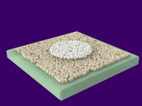
Result: A thin silver film remains where the irradiation took place.
INM-Technologie zur Abscheidung von dünnen Silberschichten und Mikrostrukturen [DE 10235803 A1, DE 102010052033 A]
BMBF funded basic research project PlaSioBio
Plasmon Resonance for Security Features, Integrated Optics and Biophotonics
In the photometallization process developed by INM, silver colloids are initially formed at a photocatalytic interface within a few 10 nm thin layer before a closed metallic film is formed upon further exposure. These colloids exhibit unique optical properties caused by surface plasmon resonance. This preliminary scientific project is aimed at enabling the technical exploitation of these properties by means of microstructuring. For example, the wavelength-dependent absorption and scattering could be used in color-selective diffraction gratings for security features. On the other hand, at wavelengths far from the resonance peak, the main expected effect is a refractive index shift, which can be used for planar waveguides and more complex integrated optical elements. Moreover, the ease of integration with metallic electrodes within the same fabrication process should also allow the realization of electro-optic modulators based on the Kerr effect. Such integrated-optical elements may be applicable for optical data communication in future fields such as autonomous mobility, but also for sensors e.g. in biophotonics.
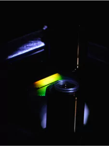
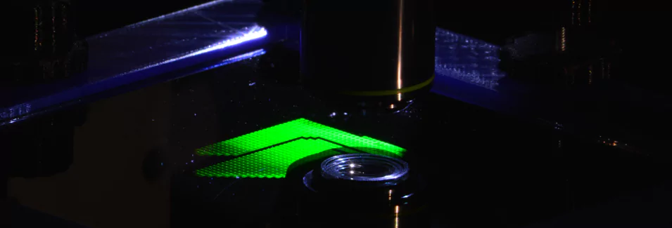
Creating a diffractive structure by writing grating elements in a field-by-field mode
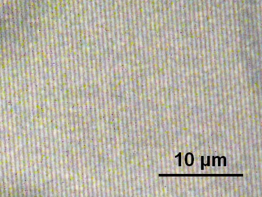
Silver colloid layer structured as a diffraction grating by double-beam interference with a grating constant of 530 nm
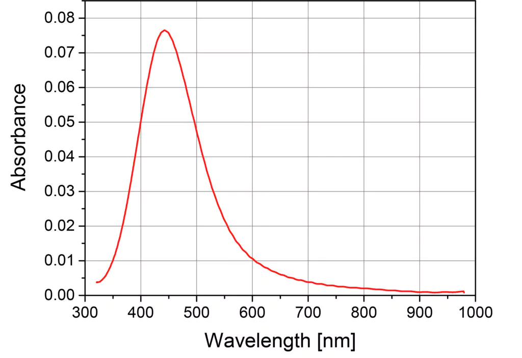
Absorption spectrum of a silver colloid layer deposited by photometallization under a transparent protective layer
Using a grating consisting of colloidal silver nano-particles to couple laser light into a planar waveguide
Plasmon Resonance for security Features, Integrated optics and biophotonics
Basic research funded by the BMBF in the „Wissenschaftliche Vorprojekte (WiVoPro): Photonik und Quantentechnologien“ scheme (December 2020 – November 2022);
Förderkennzeichen: 13N15428
https://www.photonikforschung.de/projekte/explorative-forschung/projekt/plasiobio.html
Electrospinning
New materials through targeted adjustment of the refractive index
By selectively adjusting the refractive index, interesting optical properties and effects can be used for numerous applications. If it is possible to adjust the refractive index curve of different materials over the wavelength range of visible light, then glass fibers in a polymer matrix material, for example, become invisible to the human eye. The composite appears crystal clear transparent. This is referred to as matching the dispersion curves. Examples of these systems developed at INM include coatings for holographic security markings, innovative light extraction using nanobubbles or particles as scattering centers, and highly transparent glass fiber composites for displays.
Another research topic is the development of novel photoresists for additive manufacturing using two-photon lithography to produce refractive index-matched optical polymers.
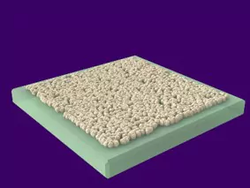
Optical nanofoams – ultrafine bubbles
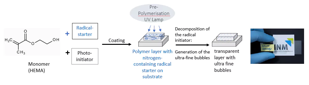
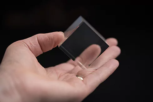
Optical nanofoams – stable dispersions of gas bubbles in the nano- and submicrometre range in transparent polymers – open up possibilities to produce novel gas-polymer nanocomposites. Due to the gas trapped in the bubbles, lightweight materials with theoretically very low refractive indices and simultaneously high transmission and low scattering are possible. Until now, these porous materials (aerogels, block copolymers or foams) have been produced by expanding supercritical CO2. INM’s innovative and proprietary approach enables the generation of nanobubbles with diameters around 60 nm in polymers. These materials with entrapped, isolated nanobubbles could find application in transparent security markings, for light extraction (for example in the medical field) or potentially as anti-reflective coatings, among other things.
The gas bubbles are generated by using azo initiators as chemical blowing agents in the transparent monomer. Depending on the application, the mixture and processing conditions must be adjusted.
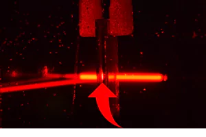
Optical nanofoams could provide novel gas-polymer nanocomposites for transparent security features through targeted process development and parameter control. The composites enable structures with a local and gradual decrease in refractive index. Coatings containing ultrafine bubbles in the embossed structure remain transparent, and the linear mask of the master embossed structure is barely visible to the naked eye. However, a linear diffraction pattern appears when red laser light is passed through the sample. The SEM images show that the embossed areas exhibit a change in microstructure and density. Ultrafine bubbles in the range of 50-100 nm were produced in the upper part of the porous PHEMA layer, while no bubbles are seen in the lower, dense region. The refractive index reduces from the dense PHEMA single layer (1.51) to the porous layer to 1.44. It is impossible to copy this information with a camera or a copying machine because the information comes from the inner microstructure. Initial experiments show that layers with embedded, structured nanobubbles also allow light to be decoupled from light guides with pinpoint accuracy.
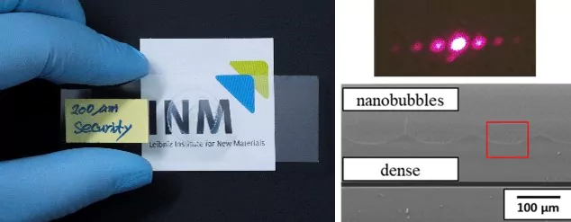
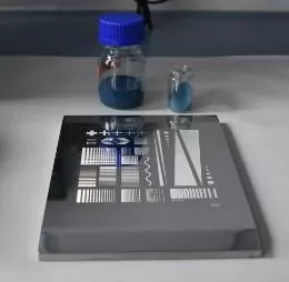
Photo of security mark with invisible optical grating (left), diffraction pattern (right, top), SEM image of cross-section of the security mark (right, down)
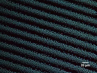
Photo of a bubbles-containing grating, created by two-wave mixing
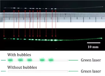
Photo of optical waveguide with nanobubbles containing light outcoupling centers
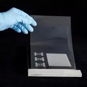
Transparent, glass fiber reinforced polymers
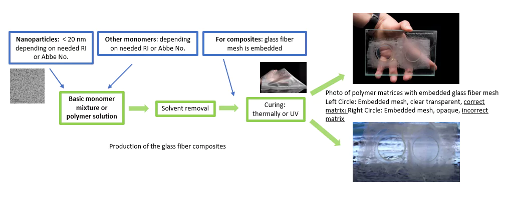
Glass fibers are already used in combination with polymers to produce transparent and lightweight materials, e.g., as light panels for roofing. By specifically combining nanoparticles and monomers, we have succeeded in adapting the dispersion curve of the plastic material to the optical properties of the glass fibers, so that the fibers become practically invisible to the human eye. These new materials have high transparency combined with flexible shaping at low process temperatures.
Refractive index matched optical polymers
In order to be able to join glass components together seamlessly and without disturbing optical impairments, for example in displays, lens systems or protective glazing “optical bonding” refractive index-adapted optical adhesives, polymer or matrix systems are essential. Every glass has different optical properties, which is why characteristic values such as dispersion curve, transmission and absorption values must first be determined. Only with knowledge of these data can the appropriate polymer system be custom synthesised. For this, suitable monomers are combined and doped with inorganic ZrO2 nanoparticles. The refractive index and Abbe number of these particles allow the tailoring of the dispersion curves.
Conventional optical polymers only cover a rather narrow range of optical properties. This is a limiting factor for the design of polymer-based optical systems, such as smartphone cameras. To overcome the limitations of conventional polymers, we developed in cooperation with the University of Stuttgart nanoinks based on the commonly used photopolymers IP-DIP and IP-S as polymer matrix and zirconia (ZrO2) nanoparticles. We show that the refractive index and dispersion of these nanoinks can be targeted by varying the ingredients and volume fraction of the nanoparticles. We also demonstrate the suitability of our nanoinks for optical applications by 3D printing individual microlenses and an achromatic Fraunhofer doublet made of several materials. The results confirm that our nanocomposites extend the range of optical properties of polymer-based systems and enable the design of high-quality, tailor-made optical materials.
Photo through a moulded polymer lense.
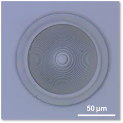
Photo of diffractive optical element 3D-printed using two photon polymerization and resist with ZrO2. (Cooperation with K. Weber and H. Gießen from 4th Physics Institute, University of Stuttgart)
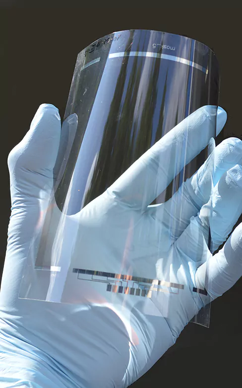
Industry Cooperations
The program division Optical Materials is interdisciplinary and has many years of experience with targeted, cooperative research and product-oriented development with partners from trade and industry. Research topics from basic research that have proven to be sustainable by appropriate market analyses are actively advertised, e.g., through trade fair appearances.
As part of a flexible project strategy, financed by funds from the industrial partners and public innovation funding, e.g., by the federal government, these basic research results are adapted and optimized in cooperation with the industrial partners to their special needs. Only this intensive cooperation with industrial partners opens up subsequent up-scaling projects by the InnovationCenter INM.
Projects
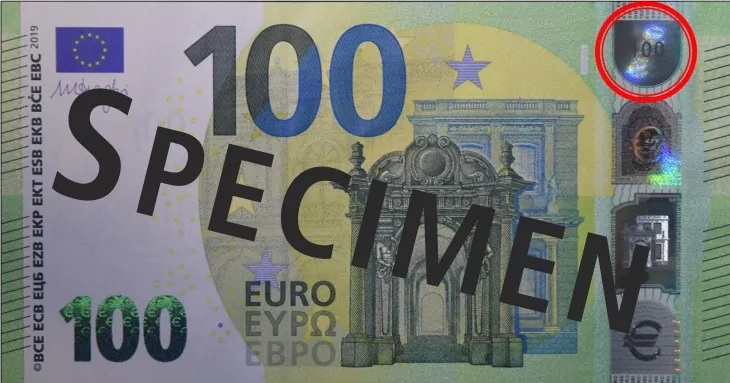
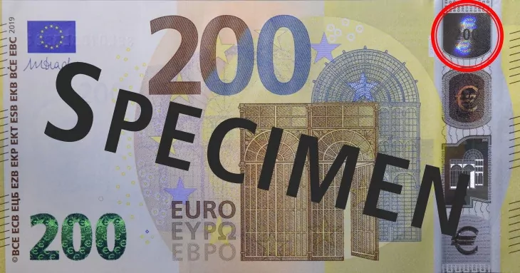
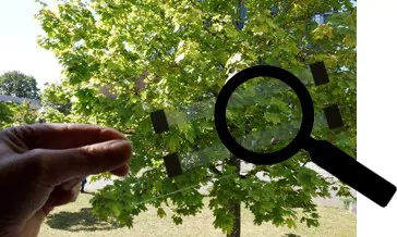
Diffractive structures for security features
Diffractive optics allow amazing optical effects in the form of holograms and related elements. As these are easy to recognize but difficult to imitate, such elements are used to secure means of payment and documents, but also high-value industrial and consumer goods against counterfeiting. Although this approach has been known for decades, several years of collaboration with SECTAGO GmbH, a start-up company from Saarland, succeeded in developing a novel technology for diffractive security features that show highly dynamic behavior under motion. Current banknotes with a security feature based on this technology have been in circulation since 2019.
Development of a galvanically enhanced photochemical layer deposition on laser-etched structures in technical glasses
Silver layers are deposited by the photometallization process developed at INM. This preliminary work served as the basis for the development of a process for the galvanic deposition of copper as part of a research project. It was possible to produce several micrometre-thick, strongly adhesive and solderable layers on various technically relevant glass substrates. The conductivity of these layers exceeds 50 % of the bulk conductivity of copper, so that, for example, sheet resistances of less than 10 mOhm/sq could be achieved with 4 µm thick layers.
By means of lithographic structuring, conductive track patterns with structure widths below 100 µm can be produced. The process is also suitable for copper-plating the inner walls of through-holes created using the laser etching technique developed by project partner Plan Optik AG. This enables complete rewiring on glass substrates and thus the production of glass-based interposers and similar assembly and module carriers for electronic components.
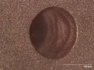
Copper-plating inner walls of
laser etched through-holes
Silver grid for electromagnetic shielding with simultaneous high transparency
Building on our work on the development of touch screen electrodes, silver gratings with simultaneously very high conductivity and high optical transparency were to be developed in order to provide optical elements with an electromagnetic shielding effect for frequencies up to the high GHz range. The close-meshed gratings required for this were produced using the photometallization process developed at INM. The required conductivity of the grids could be achieved, but the desired transparency could not yet be achieved completely. Further optimizations are the subject of ongoing research.
The illustrations present the current status: The gratings enable a very clear, transmitted image.
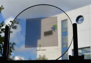
Focusing on the metal grid
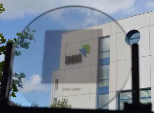
Focussing in the distance
Semi-transparent metal grid for electromagnetic shielding.
Transparent conductive layers on polymer films
In a research project at INM, transparent conductive layers on polymer film (e.g. polycarbonate, PC) were developed, which can be used as transparent electrodes for touch screens or as heating layers on car glazing. Two fundamentally suitable methods were analyzed:
Layers with silver nanowires (AgNW).
Thin polymer fibers produced by electrospinning, which are then wet-chemically metalized.
With AgNW coatings, low sheet resistivities of 9 to 15 Ohm/sq with a high transmission in the visible range of up to 88 % and a haze of approx. 2 % to 6 % are achieved.
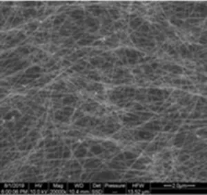
With electrospun polymer fibers, electrically conductive, transparent layers with very low sheet resistances of less than 5 Ohm/sq, a high transmission of 90 % in the visible range and a low haze of less than 2 % are realized after wet-chemical metallization. These layers can be produced at low cost and therefore offer a promising alternative to transparent conductive ITO (tin-doped indium oxide) layers used so far. Based on these metalized electrospun fibers, flexible and stretchable transparent conductive layers can also be fabricated.
SEM (scanning electron microscope) images of electrospun polymer fibers after silver coating (top) and of AgNW coatings (bottom). The diameter of the polymer fibers produced by e-spinning is 0.35 µm to several µm, and the length is up to the cm range. The AgNW have a diameter of 10 nm and a length of about 20 µm.
Screen printing pastes for the production of transparent, electrically conductive structures
New motor vehicles first placed on the market in the EU after 31 March 2018 must be equipped with an emergency call facility, the so-called “eCall function”. The antenna structures should be screen printed on the triangular side windows. However, commercially available screen-printing pastes did not fulfill the high requirement profile. Therefore, within the framework of the project (ITECA – Integration of a transparent E-Call antenna into a vehicle window), screen printing pastes were developed in the sub-project “SieTraLeit” at INM, which could be reproducibly printed to transparent layers on polycarbonate and glass. Commercial silver nanowires with lengths of approx. 30 µm and smaller and diameters of 30 and 10 nm were used to produce these pastes. The solvents used were based on the raw material exclusion list for printing inks and related products. The requirements profile was met after drying at 130 °C with sheet resistances less than 5 Ohm/sq and transmittances of 75 %.
The photo gives an impression of the transparency achievable with these pastes.
SEM photo showing the network of printed silver nanowires (right).
Projektpartner: FM Siebdruck Werbung Design GmbH;https://www.rastersiebdruck.de/
Silver nanowire based screen printing paste for transparent antenna structures
Peter König1, Ingmar Petersen2, Gabriela M. Lana1, Peter W. de Oliveira1
1 INM – Leibniz Institute for New Materials, Optical Materials, 66123 Saarbruecken, Germany; 2 FM Siebdruck Werbung Design GmbH, Research and Development, 71111 Waldenbuch, Germany
Touch sensor on polymer film
Within the framework of research and industrial projects, INM developed patterned, transparent conductive ITO (tin-doped indium oxide) layers on polymer film (e.g. PET or PC film), which can be used as transparent electrodes for touch screens.
Up to now, touchscreens are produced using sputtered ITO layers, which are patterned in a multi-stage process using etching methods, etc., which is very cost-intensive.
We designed inks from ITO nanoparticles and an adapted binder, which can be printed directly in a one-step process, for example using gravure or inkjet printing, and then be hardened by UV light.
The sheet resistance of ITO coatings is in the range of about 1 to 10 kOhm/sq after UV curing on films. Lower values of about 50 Ohm/sq are achieved after thermal treatment on glass substrates. The ITO coatings have a high transmission in the visible range of 99 %. Due to the low haze of less than 1 %, they are predestined for the cost-effective production of touch screens.

ITO nanopowder, dispersion and ink
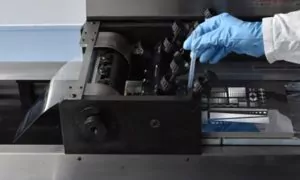
Fabrication of structured ITO layers with gravure printing machine labratester
Gravure printing plate, ITO nanopowder and ink
ITO electrodes fabricated by gravure printing for touchscreens and OLEDs
Optical sensor technology: Development of a partially backscattering coating
For applications in optical sensor technology, a coating was to be developed that was to be largely transparent to the human eye but backscatter-opaque for measurement technology. While the transmission at the measuring wavelength was to be minimized by a substrate with suitable spectral absorption characteristics, the backscattering effect was to be achieved by pigments in a transparent overcoating. In order to maximize the backscattering and at the same time maintain the optical transparency as far as possible, we developed pigments as micro-retroreflectors suitable for embedding.
At the same time, we were able to present a cost-effective alternative to the project partner: If a justifiable compromise between visual transparency and metrologically detectable backscatter is accepted, conventional microparticles of optimized size can be used.
Coating for glass substrates to increase light extraction from OLEDs
The requirements profile of our project partner specified layer thicknesses of at least 3 µm, an increased refractive index of approx. 1.8 (similar to ITO) and a short-term temperature stability of up to 250 °C. The developed layer should be crack-free, have no peak roughness, not outgas during the subsequent ITO coating and be color stable. Project-accompanying simulations by the partners made it possible to tailor the necessary specifications. In this way, the desire for coatings with scattering particles could also be met. The required low roughness was achieved by a smoothing sol. At the end of the project, two coating sols with refractive indices between 1.7 and 1.75 as well as short-term resistance at 220 °C and 250 °C were available. Various substrates of the industrial partner were coated with the developed sols. Laboratory tests confirmed the desired improvement in light extraction.
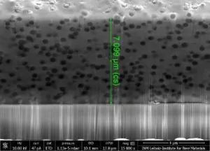
SEM image of a layer cross-section of a 7 µm thick light extraction layer with SiO2 scattering particles
Manufacturing method for silver-based antenna structures
Various methods for producing highly conductive layers were investigated with regard to their application in antenna structures. The costs were to be kept as low as possible through direct structuring during deposition and through a low layer thickness. In initial tests with the photometallization process developed at INM, it was possible to achieve sheet resistances of less than 300 mOhm/sq with layer thicknesses in the range of 100 nm. Alternatively, the use of the project partner’s available printing technologies was investigated. Modified ink formulations known from literature in combination with engraving printing also achieved high conductivities with shorter process times, but with the disadvantage of a higher material input.
Optical filters: Transparent neutral grey layers on glass
Optical filters for camera systems are usually made of colored or coated glass using complex vacuum processes (CVD, PVD). In cooperation with our industrial partner, this project realized the production and application of neutral grey, transparent coatings with low haze and uniform transmission values in the wavelength range of 450-650 nm on glass, which is particularly sensitive to the eye. The process of wet chemical coating with sol-gel using colored nanoparticles is cost-effective and simple.
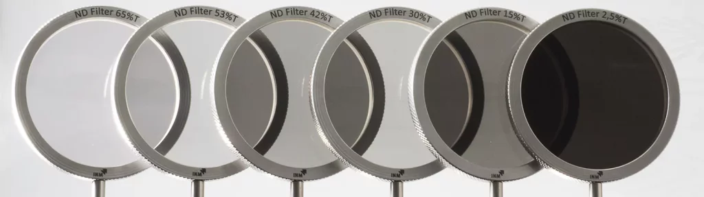
Filter with neutral grey transparent coating on glass substrates (transmission 65 % – 2.5 %)
Neutral photochromic intraocular implant (IOL)
Modern cataract surgery makes it possible to replace the clouded lens with an intraocular plastic implant – however, increased glare sensitivity remains. We developed a reversible neutral photochromic material suitable for flexible and foldable intraocular lenses (IOLs) for automatic, dynamic brightness control after cataract surgery. Taking biocompatibility into account, broadband absorbing pyrans were subsequently incorporated via the thermal transfer process or directly during polymerization via the mass staining process. The starting material was limited to swellable, hydrophilic acrylate systems. During mass dyeing, thermal co-polymerizations led to high-quality photochromic molded bodies, which were processed into IOLs by the project partner using established mechanical production processes. After swelling of the material, the photochromic effect is even more intense than in the dry state. The basic suitability of the material was demonstrated. Further material optimization and adaptation of the long-term stability of the photochromic effect are still pending.
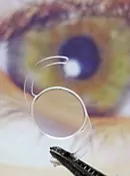
IOL in front of a human eye
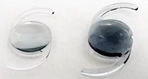
Reversible photochromic IOLs: Comparison of a dry, non-UV-activated photochromic IOL (left) with an identical but swollen and UV-activated photochromic IOL (right).
Project partners

ZIM-Koop-Projekt
Träger AIF Projekt GmbH
Förderkennzeichen KF2024304MD2
Downloads
- Handout: Photometallization – New touchscreens
- Handout: Transparent glass fiber reinforced polymer
- Handout: Diffusion barrier and sodium ion supplying flexible sol-gel layer for cigs solar cells
- Handout: Electrospun flexible transparent electrodes
- Handout: Printed transparent conductive oxide coatings and patterns
Publications
Bhusari, Shardul | Hoffmann, Maxi | Herbeck-Engel, Petra | Sankaran, Shrikrishnan | Wilhelm, Manfred | del Campo, Aránzazu
Soft Matter , 2023, 20 (6), 1320-1332.
https://pubs.rsc.org/en/Content/ArticleLanding/2024/SM/D3SM01119D
Zolotukhina, E. V. | Butyrskaya, E. V. | Koch, Marcus | Herbeck-Engel, Petra | Levchenko, M.G. | Silina, Yulia E.
Physical Chemistry Chemical Physics , 2023, 25 (14), 9881-9893.
https://doi.org/10.1039/D3CP00829K
Gießelmann, Elias C. J. | Engel, Stefan | Kostusiak, Weronika | Zhang, Yuemei | Herbeck-Engel, Petra | Kickelbick, Guido | Janka, Oliver
Dalton Transactions , 2023, 52 3391-3402.
https://doi.org/10.1039/D3DT00141E
Kócs, Lenke | Jilavi, Mohammad H. | Beckelmann, Dirk | Schäfer, Bruno | May, Alexander | Koch, Marcus | de Oliveira, Peter W.
Ceramics International , 2021, 48 (3), 4165-4171.
https://www.sciencedirect.com/science/article/pii/S0272884221033514
Kócs, Lenke | Jilavi, Mohammad H. | Koch, Marcus | Oliveira, Peter William de
Ceramics International , 2020, 46 (16, Part A), 25865-25872.
http://www.sciencedirect.com/science/article/pii/S0272884220320691
Prieto-López, Lizbeth Ofelia | Herbeck-Engel, Petra | Yang, Li | Wu, Qian | Li, Juntang | Cui, Jiaxi
Advanced Materials Interfaces , 2020, 7 (18), 2000876.
https://onlinelibrary.wiley.com/doi/abs/10.1002/admi.202000876
Feng, Jun | Jiang, Qiyang | Rogin, Peter | Oliveira, Peter William de | del Campo, Aránzazu
ACS Applied Materials & Interfaces , 2020, 12 (18), 20287-20294.
https://doi.org/10.1021/acsami.0c03903
Weber, Ksenia | Werdehausen, Daniel | König, Peter | Thiele, Simon | Schmid, Michael | Decker, Manuel | Oliveira, Peter William de | Herkommer, Alois | Giessen, Harald
Optical Materials Express , 2020, 10 (10), 2345-2355.
http://www.osapublishing.org/ome/abstract.cfm?URI=ome-10-10-2345
Ababneh, A. | Albataineh, Z. | Dagamseh, A. M. K. | Al-kofahi, I. S. | Schäfer, Bruno | Zengerle, T. | Bauer, K. | Seidel, H.
Thin Solid Films , 2019, 693 137701.
http://www.sciencedirect.com/science/article/pii/S004060901930728X
Purtov, Julia | Rogin, Peter | Verch, Andreas | Johansen, Villads Egede | Hensel, René
Nanomaterials , 2019, 9 (10), 1495.
https://www.mdpi.com/2079-4991/9/10/1495